

REQUEST DEMO
Robot CATALOG will be sent to your mailbox immediately after submission.
SUBMIT
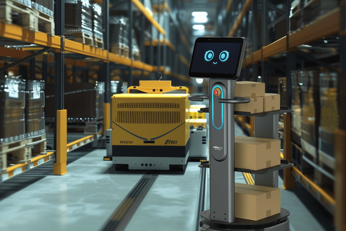
Operating within the ultra-strict environments of cleanrooms, semiconductor fabs face mounting material handling challenges, including a chronic shortage of workers willing to perform physically demanding shifts in full bunny suits, the high cost of wafer damage from manual transport, and the strict contamination compliance required for next-generation yields. As wafer sizes grow and the financial stakes of human error multiply, Industrial AMRs have emerged as a critical solution to automate wafer transport, reduce human-borne particulates, and maintain the continuous, highly reliable material flow essential for modern semiconductor manufacturing.
The OrionStar CarryBot D150 Cleanroom Edition provides a practical example of how these autonomous capabilities are deployed in high-tech manufacturing environments. According to manufacturer specifications, the unit utilizes VSLAM+ navigation combined with LiDAR and depth vision sensors to operate in spaces with a minimum passage clearance of just 65 cm, which is highly relevant for navigating constrained cleanroom aisles. It features a net payload capacity of up to 150 kg, allowing it to transport multiple heavy wafer carriers simultaneously while managing uninterrupted workflows via an automatic charging dock and a battery life of up to 12 hours under tested conditions. By incorporating a five-layer safety protection system, the platform safely executes autonomous material transfers without requiring fixed layout modifications.
These long, connecting corridors are essential for moving materials between different cleanroom bays, but they demand constant, repetitive walking from cleanroom staff. Industrial AMRs take over these high-frequency, cross-floor transportation routes, freeing human workers from exhausting manual labor while maintaining a steady, reliable flow of wafer carriers.
Wafer stockers act as critical buffering zones where front-opening unified pods (FOUPs) are temporarily held before entering the process tools. Autonomous platforms interface directly with these intelligent buffering stations to seamlessly retrieve and deposit heavy cassettes, ensuring the tools are never starved for materials and minimizing operator intervention.
In older brownfield fabs, equipment staging zones are often characterized by tight aisles and clustered layouts that cannot accommodate fixed monorail systems. AMRs navigate these constrained, dynamic environments using advanced spatial mapping and obstacle avoidance, delivering components safely without requiring the facility to tear down existing infrastructure.
Transporting empty carriers, waste materials, or rejected wafers back to designated return areas is a non-value-added task that historically consumed valuable operator time. Mobile robots can be scheduled to execute these reverse logistics routes autonomously, keeping the active production floor clear of clutter and allowing technicians to focus strictly on yield-critical operations.
For Industrial AMRs to function effectively in a semiconductor fab, they must be seamlessly integrated into the facility's existing Material Control System (MCS) and Manufacturing Execution System (MES). Rather than operating as isolated units, these robots communicate directly with the fab's broader Automated Material Handling Systems (AMHS) and production planning software to coordinate scheduling, predict tool congestion, and adapt routing in real time. Through standardized interfaces like the SEMI E82 specification and barcode or RFID-based WIP identification, the robotic fleet ensures that every material movement is logged and orchestrated, serving as the flexible transport layer that bridges overhead hoists (OHT) and intelligent stockers.
Industrial automation is proving to be a vital asset in advancing the semiconductor industry's commitment to both environmental sustainability and the long-term well-being of its workforce.
Industrial AMRs are fundamentally changing the way Semiconductor Fabs manage and maintain material flow within Cleanrooms, shifting the focus from manual labor to precision automation and continuous reliability. By addressing structural pain points like ergonomic strain, particulate contamination, and layout constraints, these platforms ensure that highly valuable wafers are moved safely and efficiently. With solutions like the OrionStar CarryBot series offering various configurations to adapt to different payload and spatial requirements, facility operators have the flexible tools necessary to modernize their intralogistics and meet the demanding standards of next-generation semiconductor manufacturing.